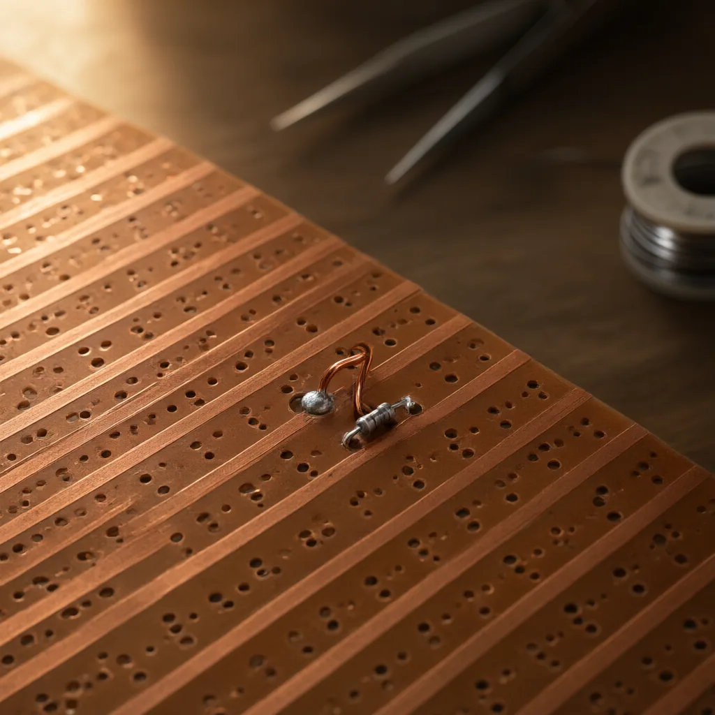
A stripboard layout becomes much easier to follow once you stop seeing it as a picture and start reading it as a map of copper paths, breaks, and wire links. This guide is for pedal builders, electronics beginners, and anyone moving from a schematic to a practical build on veroboard or stripboard. The goal is simple: identify what each mark means before you cut, solder, or troubleshoot.
What the copper strips are doing
Stripboard has parallel copper tracks running along one side of the board, with evenly spaced holes that let components pass through from the other side. Each continuous strip behaves like an electrical connection point shared across multiple holes. If a resistor lead, capacitor lead, and transistor pin all enter the same uninterrupted strip, they are electrically joined unless the strip is deliberately cut.
That is the key difference from a printed PCB layout: stripboard starts as a set of long connected rails, and you shape the circuit by deciding where those rails should stop and where new connections should be added.
How to read cut points
In most stripboard diagrams, highlighted squares or marked holes indicate cut points. These are places where the copper strip must be broken so the connection does not continue down the full length of the board. A cut point is not decoration or a drill guide; it changes the circuit.
Before making a cut, confirm three things:
1. The mark sits on a copper strip, not an empty mounting position. 2. The break is required to isolate two sections that would otherwise be shorted together. 3. The location matches the row and column used by the surrounding components.
A sharp hand tool made for controlled cutting is usually easier to manage than twisting a large drill bit by hand. After cutting, inspect the copper closely under good light. A partial ring left behind can create an intermittent fault that is hard to spot later.
What the wire links mean
Many layouts use straight black lines or similar marks to show wire links. These are added jumpers, often made from solid bare or insulated wire, that connect points the original copper strips do not connect on their own. Think of them as custom bridges placed on top of the stripboard plan.
Some links run vertically across several strips, while others make short local hops. Their job is usually one of three things: crossing signal paths, bringing power to another section, or reconnecting nodes that were separated by necessary cut points. When reading the diagram, treat each link as a deliberate conductor with two endpoints that must land exactly where shown.
A reliable way to check the layout before soldering
Start by orienting the board so the strip direction matches the diagram. Then mark all cut points first, verify them, and only cut when the full pattern makes sense. Next place wire links, because they are easier to confirm on an uncluttered board. After that, install low-profile parts such as resistors and diodes, followed by taller components.
If the layout is for an audio effect or small analog circuit, pause before powering it and continuity-check the board with a multimeter. Confirm that every intended strip is continuous, every cut point is truly open, and adjacent strips are not accidentally bridged by solder.
Common reading mistakes that cause build errors
The most frequent problems are reading the strip direction backward, missing a single cut point, or assuming a wire link is just a drawing aid. Builders also sometimes count holes from the wrong edge, which shifts a component by one row and changes the whole connection pattern.
When in doubt, compare the finished board against the diagram one electrical node at a time rather than one component at a time. That method is slower, but it matches how the circuit actually behaves and makes troubleshooting far more efficient.